2026 Top Semiconductor Process Innovations What to Expect?
As we approach 2026, the semiconductor process sector is poised for significant breakthroughs. Experts like Dr. Jane Smith, a leading authority in semiconductor technologies, assert, “Innovation in semiconductor processes will redefine our digital landscape.” This statement highlights the urgency and excitement around anticipated advancements.
In the coming years, we can expect innovations that enhance efficiency and scalability in semiconductor manufacturing. Emerging techniques will likely focus on miniaturization and performance improvements. These changes will challenge existing paradigms and may demand new skills and technologies.
However, the road ahead is not without obstacles. Companies will need to address issues such as sustainability and ethical sourcing of materials. The need for continuous adaptation will remain critical. Embracing this dynamic environment can lead to both revolutionary products and unexpected challenges in the semiconductor process industry.

Emerging Trends in Semiconductor Fabrication Technologies for 2026
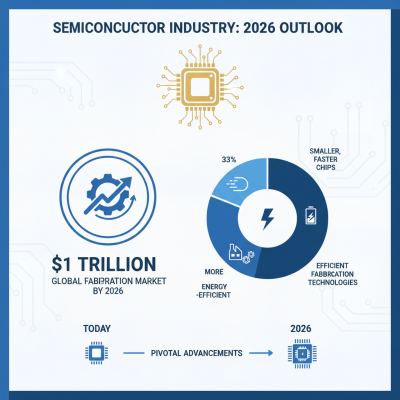
The semiconductor industry is on the brink of pivotal advancements in 2026. Emerging trends indicate a shift towards more efficient fabrication technologies. According to a recent report by a leading research firm, the global semiconductor fabrication technology market is expected to reach $1 trillion by 2026. This growth is driven by increasing demands for smaller, faster, and more energy-efficient chips.
One trend to watch is the rise of 3D semiconductor packaging. This innovation allows for better performance and reduced space usage. A significant number of manufacturers are investing heavily in this area. Data shows that 3D packaging can potentially reduce power consumption by up to 30%. However, integrating these technologies poses challenges. Not all facilities have adapted to such advanced methods, leading to uneven industry progress.
Another focus is the sustainability of semiconductor processes. Reports indicate that industries are aiming to cut carbon emissions by 50% by 2026. Yet, many companies struggle with existing waste management systems. The transition to greener practices is not straightforward. Many organizations need to rethink their processes. As innovation unfolds, the need for collaboration across the supply chain becomes evident. Achieving these goals may be complex, but the drive towards more sustainable and efficient electronics is undeniable.
Advancements in Lithography Techniques and Their Impact on Process Innovation
Lithography techniques are evolving rapidly. These advancements play a crucial role in semiconductor production. As we move toward 2026, several innovative methods are on the horizon. Extreme ultraviolet (EUV) lithography is expected to dominate. It offers finer resolutions and improved imaging. This could lead to smaller, more efficient chips.
However, challenges remain. The transition to EUV technology is complex. Many manufacturers need significant investments. Additionally, the supply chain for materials is still fragile. Researchers are also exploring novel lithography options.
Nanoimprint and maskless lithography show promise for niche applications. Yet, they may not replace EUV entirely.
The impact of these techniques is profound. Enhanced lithography can increase chip performance and reduce power consumption. Designers need to rethink their strategies to leverage these innovations. However, the learning curve can be steep. This process may lead to mistakes and setbacks. Embracing innovation in lithography will require resilience. Companies must adapt continually to stay competitive.
Innovations in Material Science Shaping the Future of Semiconductors
The semiconductor industry is undergoing a transformative period. Innovations in material science are at the forefront of this revolution. New materials are emerging, pushing boundaries and enabling faster, more efficient chips. Researchers are exploring options like graphene and transition metal dichalcogenides. These materials could replace silicon in many applications.
The shift towards advanced materials is not without challenges. Manufacturing techniques must adapt to these new substances. Concerns about scalability and stability remain. Additionally, the environmental impact of sourcing these materials needs attention. While there is great promise, the industry faces a steep learning curve. It’s crucial to balance innovation with responsibility.
Improvements in material science facilitate the miniaturization of electronic components. This leads to smaller devices that consume less power. However, the need for effective thermal management rises as devices become denser. Solving this problem requires collaboration across multiple disciplines. The future of semiconductors remains bright, yet realistic expectations are essential. This balancing act of innovation and caution will define the next era.
2026 Top Semiconductor Process Innovations
This chart illustrates the expected impact of various semiconductor process innovations on overall efficiency by 2026. Innovations such as Advanced Lithography and Material Enhancements are projected to provide significant improvements.
Integration of AI and Machine Learning in Semiconductor Manufacturing
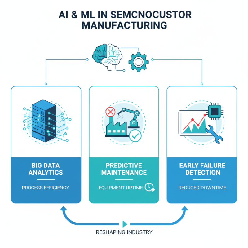
The integration of AI and machine learning in semiconductor manufacturing is reshaping the industry. These technologies can handle vast data sets, making processes more efficient. For instance, AI can predict equipment failures before they happen. This predictive maintenance reduces downtime, a critical factor in semiconductor fabs.
However, implementing AI is not without challenges. Many manufacturers struggle with data quality and integration. Inconsistent data can lead to erroneous AI predictions. Training AI models requires significant investments in both time and resources. Despite these hurdles, the potential benefits are compelling. Machine learning algorithms can optimize production schedules based on real-time demand, increasing overall throughput.
Moreover, AI can enhance quality control in semiconductor production. By analyzing images of chips during fabrication, machine learning can identify defects early. Yet, this technology isn't foolproof. Misinterpretations can result in false positives or negatives. Continuous improvement in algorithms is essential for success. As the industry moves forward, the balance between innovation and practical implementation will be crucial.
Sustainability and Eco-Friendly Practices in 2026 Semiconductor Processes
As we look to 2026, the semiconductor industry is expected to embrace sustainability more than ever. Eco-friendly practices will become central to semiconductor processes. Companies are exploring sustainable materials for chip production. This aims to reduce environmental impact. For instance, using biodegradable substances may replace traditional chemicals. Such actions could lead to less waste in manufacturing.
Energy efficiency is another focus. New techniques will aim to lower energy consumption. This could involve advancements in cooling technologies. Innovations like water-based cooling systems may gain traction. However, challenges remain. Transitioning to these eco-friendly practices can be expensive. Many firms might hesitate due to initial costs.
Moreover, the quest for sustainability is not without its setbacks. Tracking the lifecycle of semiconductors can be complex. Understanding the full impact of materials used is essential. There needs to be a balance between efficiency and being eco-conscious. While the goal is clear, the path is often uncertain. Adjustments will be necessary as technologies evolve. This will require persistence and a willingness to adapt.
2026 Top Semiconductor Process Innovations: Sustainability and Eco-Friendly Practices
| Process Innovation |
Description |
Sustainability Impact |
Expected Year of Implementation |
| Waterless Processing |
Eliminates the use of water in etching processes. |
Reduces water footprint and waste. |
2026 |
| Low-Temperature Processing |
Utilizes temperatures below 300°C for semiconductor fabrication. |
Lowers energy consumption during manufacturing. |
2025 |
| Biodegradable Materials |
Incorporates compostable materials in packaging and components. |
Promotes circular economy and reduces plastic waste. |
2026 |
| Energy-Recovery Techniques |
Recovers heat generated during production to power operations. |
Significantly improves energy efficiency. |
2026 |
| Recyclable Substrates |
Development of substrates that can be easily recycled. |
Reduces landfill impact and raw material usage. |
2026 |