Top Semiconductor Process Techniques You Should Know?
The semiconductor process industry is continuously evolving, with techniques that significantly influence technology development. Dr. Lisa Chen, a leading expert in semiconductor manufacturing, once stated, "Understanding semiconductor processes is key to driving innovation." This highlights the importance of mastering various techniques in this field.
In recent years, critical advancements have emerged. Processes like photolithography and etching define how tiny circuits are created on silicon wafers. The precision required in these methods is extraordinary. Small errors can lead to significant defects, ultimately impacting device performance.
However, many professionals struggle with these complex techniques. The learning curve is steep, and mistakes can be costly. Continuous training is essential. As technology progresses, staying updated on new methodologies becomes vital for success.
Overview of Semiconductor Manufacturing Processes
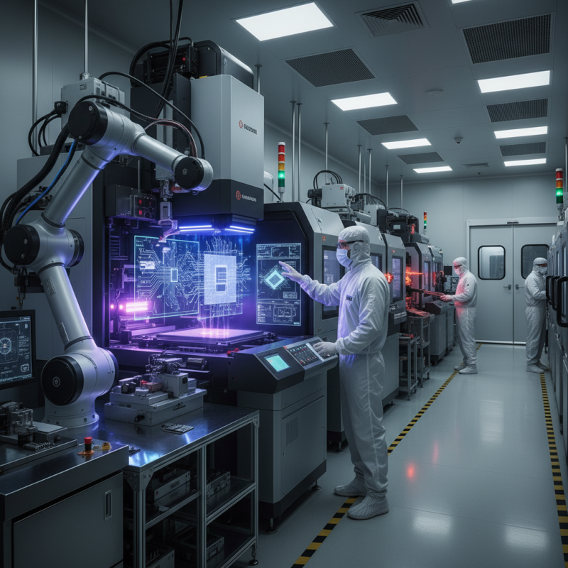
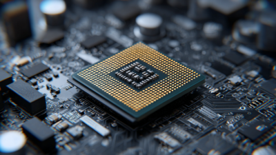
Semiconductor manufacturing is a complex process. Many steps occur in a cleanroom environment to ensure precision. Each process impacts the final product's quality, efficiency, and cost. A recent report indicates that the global semiconductor market reached $500 billion in 2022, highlighting the industry's rapid growth. As demand soars, optimizing manufacturing techniques becomes crucial.
Photolithography is key in creating intricate circuits. It uses light to transfer patterns onto semiconductor materials. This process requires precise control over light wavelengths and exposure times. Recent advancements in Extreme Ultraviolet (EUV) lithography have allowed manufacturers to more accurately produce smaller features. However, EUV systems can be incredibly costly. Many smaller manufacturers struggle to invest in this technology.
Etching follows lithography, further defining circuit elements. Different etching techniques like dry and wet etching affect material properties. Studies show that selecting the right etching method can reduce defects and improve yield by 10-15%. However, challenges like chemical waste management persist. Engineers often seek methods that balance effectiveness and environmental impact.
Top Semiconductor Process Techniques You Should Know
Key Photolithography Techniques in Semiconductor Production
Photolithography plays a crucial role in semiconductor production. It is the process used to create intricate circuit patterns on silicon wafers. A mask with the desired design is placed over a photoresist-coated wafer. Ultraviolet light then transfers the pattern onto the photoresist. This is a precise and highly controlled method. Yet, it requires constant adjustments and refinement.
One effective tip is to maintain an optimal environment. Temperature and humidity can significantly affect the process. Even small fluctuations can lead to imperfections. Regularly cleaning equipment is also vital. Dust particles can ruin the delicate patterns. So, check your workspace frequently.
Another aspect to consider is the choice of materials. Using high-quality photoresists can make a difference. Some materials may perform better under specific conditions. However, experimenting with new substances can be risky. It may lead to unexpected results. It’s essential to document each trial for better insights. This way, you can make informed decisions while fine-tuning your process.
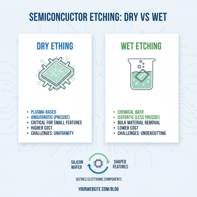
Etching Methods: Dry vs. Wet Etching Explained
Etching is a vital process in semiconductor manufacturing. It defines features on silicon wafers, shaping the electronic components we rely on. There are two main etching methods: dry etching and wet etching. Each has unique advantages and limitations.
Dry etching uses gases to etch materials. The precision it offers is remarkable. A report from the Semiconductor Industry Association reveals that advanced dry etching techniques have increased pattern resolution by up to 30%. This improvement is crucial for creating smaller, more efficient transistors. However, the process may lead to issues such as unwanted residues on the wafer.
Wet etching, on the other hand, involves chemical solutions to remove material. It's generally simpler and less expensive than dry etching. This method is still widely used for bulk material removal. However, it can lack the precision of its dry counterpart. This leads to challenges in maintaining strict feature dimensions. According to recent studies, wet etching might not meet the evolving demands of nanoscale fabrication. Each technique has strengths but also room for improvement. Understanding these nuances can guide better choices in semiconductor processes.
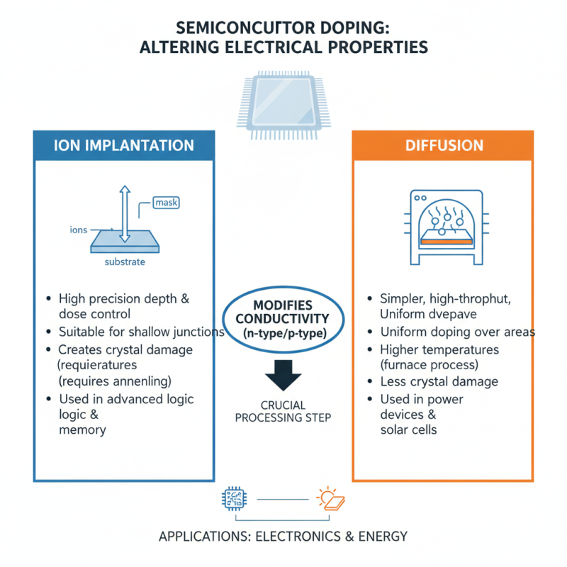
Doping Techniques: Ion Implantation and Diffusion
Doping is a crucial step in semiconductor processing. It alters the electrical properties of materials. Two main techniques are ion implantation and diffusion. Each has its advantages and specific applications.
Ion implantation is precise. It places ions directly into the substrate. This control allows for shallow doping profiles. However, it can also introduce damage to the silicon lattice. This damage may require additional annealing processes to repair.
Diffusion, on the other hand, is a simpler method. It involves placing a dopant source in contact with the substrate. The dopants then diffuse into the material through heat. While diffusion is easier, it lacks the precision of ion implantation. This can lead to variations in dopant concentration.
**Tips:** When selecting a technique, consider your project's requirements. Analyze the trade-offs between depth, precision, and damage. Always reflect on the implications of your choices. Testing can reveal unexpected results. Don't overlook the need for refinement in both methods.
Advancements in Cleanroom Environments for Chip Fabrication
The cleanroom environment is crucial for semiconductor fabrication. These controlled spaces help minimize contamination. A recent report highlighted that 90% of defects arise from particles in the air. Maintaining ultra-clean environments is essential for chip performance.
Advancements have improved cleanroom technology. New filters and air circulation systems can reduce particle counts significantly. Studies show that maintaining a particle count below 100 particles per cubic foot can enhance yield rates. However, it requires constant monitoring and adjustments. This raises questions about the cost-effectiveness of such rigorous standards.
Despite progress, challenges remain. Equipment calibration is often overlooked, leading to inconsistencies. Human error in cleanroom protocols can also result in defects. Addressing these issues is vital for the future of semiconductor manufacturing. Companies must continuously adapt to achieve the highest standards in cleanroom environments.
Top Semiconductor Process Techniques You Should Know
| Process Technique |
Description |
Advantages |
Challenges |
| Photolithography |
A process used to transfer patterns onto a substrate. |
High precision, ability to produce intricate designs. |
Limited by optical diffraction and resolution. |
| Etching |
Chemical or physical removal of material from the substrate. |
Allows for selective material removal, creating patterns. |
Can be difficult to control, leading to defects. |
| Deposition |
Process of depositing thin films onto surfaces. |
Versatile for various materials, including metals and insulators. |
Thickness uniformity and adhesion issues can arise. |
| Chemical Mechanical Planarization (CMP) |
Process combining chemical and mechanical actions to smooth surfaces. |
Improves surface flatness, which is critical for multiple layer structures. |
Can introduce new defects if not carefully managed. |
| Ion Implantation |
Technique used to dope semiconductors with impurities. |
Highly controlled doping levels, leading to better device performance. |
Can create defects in the crystal structure. |